knowledge
Basic switching principle of IGBT
The basic switching principle of IGBT is reflected in the interaction between unipolar MOS gate structure and bipolar PNP transistor. Refer to the basic structure and equivalent circuit shown in Figure 1.
IGBT equivalent circuit
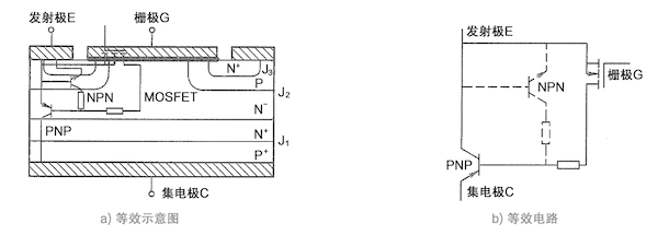
Figure 1 IGBT equivalent circuit
01 conduction of IGBT
When the IGBT is in forward bias and blocked, when the gate emitter voltage is higher than the turn-on voltage of the MOS structure, and the strong inversion layer on the surface of the p region below the gate in the MOS structure forms a conductive channel, the IGBT will enter the forward conduction state. At this time, electrons can enter the N region through the channel from the N + region connected with the emitter, which is equivalent to providing electron flow for the base of PNP transistor. At the same time, due to the positive bias of the j 1 junction, the P + region will inject holes into the N region, some of which will compound with electrons, and some of which will enter the emitter of the IGBT (exactly the collector of the PNP transistor) through the electric field of the j 2 junction. At this time, there is current in the whole IGBT, and the IGBT is on. In the N region, electrons and holes accumulate to form conductance modulation effect.
On state of 02 IGBT
The current capacity of IGBT in on state is affected by both grid voltage and Collector Emitter positive bias, and the physical mechanism is affected by the monopole and bipolar conductivity. When the positive Collector Emitter bias of IGBT increases, the injected hole density of the positive collector biased PN junction increases correspondingly, until it exceeds the multi carrier concentration at equilibrium in the N region. In this way, as long as the gate voltage is high enough to make the conduction channel open wide enough, the on state voltage current characteristics of IGBT are not much different from that of PIN diode. Even if the rated blocking voltage is very high, the current capacity can reach a very high level, and the bipolar device has more characteristics. However, in the case of low gate voltage, due to the insufficient conductivity and high resistance of the conductive channel of the inversion layer, the applied voltage will mainly fall in this region, and the voltage current of IGBT will show the saturation characteristics as the general MOSFET. There are more monopolar conducting behaviors. These two interactions interact to form the output characteristics shown in Figure 2.
Figure 2 shows the saturation region dominated by the characteristics of the unipolar MOS structure and the active region dominated by the characteristics of the transistor. When the current increases and the voltage between collector and emitter increases to a certain extent, the transistor part undertakes the main part of the IGBT current, so that the MOSFET part of the current will not continue to enter the saturation state, so the current saturation in IGBT is also called sub saturation And.
03 IGBT shutdown
For the IGBT which is in the forward bias and on state, if you want to turn it into the off state, just let the gate voltage UGS < ut. A simple way is to realize it through the gate and emitter short circuit. When UGS drops to zero, the P-region surface in MOS gate structure can no longer maintain the inversion state, the conductive channel disappears, the electron supply from emitter to n-base region is cut off, and the turn off process begins. When IGBT is on, P + region injects minority carrier holes into n region. These minority carriers diffuse to J2 junction and store a certain capacity of carriers in N region. Like any bipolar device, the forward conduction process of IGBT can not be finished immediately. It takes some time for these minority carriers to disappear through recombination and sweeping, that is, the collector current needs some time to gradually decay.
Hold up effect of parasitic thyristors in 04 IGBT
The above analysis shows that the on state and off state of IGBT are the result of the condition that the parasitic thyristor does not work. In practical application, the parasitic thyristors of IGBT can be divided into two types: the parasitic thyristors of IGBT and the parasitic thyristors of IGBT
Static holding effect
The static hold up effect occurs in the on state of IGBT. The key is whether the equivalent NPN transistor in IGBT has positive feedback with PNP crystal. In the equivalent circuit, an equivalent body area resistor is paralleled between the base and emitter of NPN transistor. When the current flows through the equivalent body area resistance and produces a voltage drop, it is equivalent to adding a forward bias voltage to the base of NPN transistor. Within the specified collector current range, the forward bias voltage is not large enough, so the NPN transistor will not turn on. However, when the collector current of IGBT increases to a certain value, the forward bias voltage will make the NPN Transistor turn on and excite each other with the PNP transistor, forming a current positive feedback phenomenon similar to that when the thyristor turns on inside the two transistors. The current amplification multiple α of the two transistors increases with the increase. When the sum of the two transistors is greater than 1, the thyristor hold up effect occurs, that is, in IGB There is a current path between the collector and emitter of T, which does not depend on external excitation and makes the device out of control, which is called static hold up effect.
Dynamic holding effect
The dynamic hold up effect occurs in the transient process of IGBT turn off or device short circuit. In the process of IGBT turn off, it is inevitable that the terminal voltage between collector and emitter rises rapidly, and the high Du / dt causes the NPN transistor base to input large displacement current and turn on, which is one of the reasons for the parasitic thyristor to trigger on. When the channel pinch off of MOS gate structure is very fast, the space charge of J2 junction is built up quickly, the displacement current is large, and it is easy to trigger the parasitic thyristor on. The dynamic hold up effect is mainly determined by the rate of voltage change, collector current and junction temperature. The collector current allowed by dynamic holding effect is smaller than that allowed by static holding effect.
05 positive blocking of IGBT
When the IGBT is in the positive bias, that is, the IGBT collector is connected to the positive potential, and the emitter is connected to the negative potential. When the gate emitter voltage is lower than the turn-on voltage of MOS structure, the collector PN junction is positively biased and has no contribution to blocking, so the forward blocking principle of IGBT is similar to that of VDMOSFET. Because there is no channel in MOS gate structure, it can not supply current to the base of PNP transistor. The whole IGBT can be regarded as a PNP transistor without base current, which is in the blocking state. If we consider the effect of parasitic thyristor, it can also be regarded as a thyristor without gate trigger. At this time, we need to avoid other conditions to trigger the thyristor. The forward blocking voltage capability of IGBT is mainly determined by the avalanche breakdown voltage of J2 junction. The forward bias of IGBT is shown in Figure 3. When the forward voltage exceeds the threshold voltage, breakdown occurs.
06 reverse blocking of IGBT
When IGBT is reversely biased, the PN junction of collector is reversely biased, and the existence of J1 junction makes IGBT have the ability to withstand reverse voltage, which is different from MOSFET. When moseet is reversely biased, it will show the diode characteristics of forward bias, and has no reverse blocking ability. However, in IGBT, designers usually sacrifice large reverse blocking capability in exchange for low conductivity and low turn off loss. Therefore, the reverse breakdown voltage of J1 junction is low, and the reverse blocking ability of IGBT is not high. IGBT reverse bias is shown in Figure 4.
In many voltage type power electronic converters, independent anti parallel diodes are added to IGBT to meet the needs of converter commutation, and the graphic symbols of the formed reverse conduction devices are shown in Fig. 5A; in some current type power electronic converters or matrix converters, if IGBT is required to have good reverse blocking ability, independent diodes are connected in series in IGBT to form Fig. 5B Figure symbol of reverse resistance device shown in.
Latest News
Contact Us
Email:info@dynpower.cn
Add:No. 77, Louyang Road, Suzhou Industrial Park
 qq
qq