knowledge
Basic structure of IGBT
As an important power semiconductor device in power electronic converter, insulated gate bipolar transistor (IGBT) has been growing for several years, because it makes power electronic converter devices and equipment achieve higher efficiency and miniaturization. This means that the application field of IGBT has been extended to a wide range, not only in industry, but also in many other power conversion systems, it has replaced the power bipolar transistor (BJT) and power MOSFET. In the high voltage and large capacity power electronic converter, it has a situation of full control power semiconductor devices with IGCT and thyristor.
IGBT is a typical unipolar and bipolar hybrid device. Which part of IGBT is dominant has different understanding in different periods and different devices. According to different cognitive levels of IGBT, there have been many naming methods since its invention, such as insulated gate transistor (IGT) and conductivity modulated field effect transistor (comfet). It was not until the late 1980s that the naming method of IGBT was recognized by everyone. It is generally believed that IGBT is a hybrid power semiconductor device evolved from the combination of MOS gate structure and bipolar transistor. Therefore, the use of IGBT has the dual characteristics of bipolar transistor and power MOSFET, thus forming a better compromise (between on state voltage drop and switching time), a lower total loss (the sum of on loss and switching loss) and a more stable switching safe working area (SOA). Therefore, IGBT has the comprehensive advantages of good control ability of insulated gate and on-state conductivity modulation.
IGBT was put on the market in the early 1980s. At that time, there were some problems, such as poor parallel operation due to poor temperature characteristics of devices, poor turn off due to more carrier accumulation in the body, and limited operation area due to the holding effect of parasitic thyristors in the body. With these problems gradually solved, IGBT began to be widely used, and its advantages as a hybrid device are more and more reflected The more obvious.
IGBT can be considered to be evolved from VDMOSFET. Compare the structure of VDMOSFET with the original IGBT concept, as shown in Figure 1. It is not difficult to see that the top half of the two devices are basically the same, but there is a significant difference in the bottom half: IGBT has one more p + layer than VDMOSFET, so there is one more large area PN junction. The basic starting point is to introduce a drain side PN junction into the VDMOSFET structure to provide forward injection of minority carriers to achieve conductance modulation and reduce the on-state voltage drop.
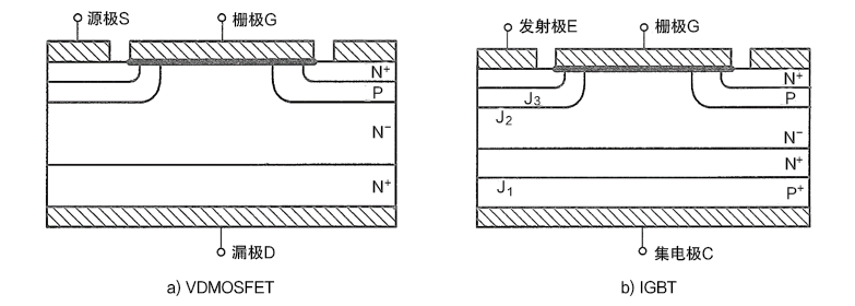
Figure 1 structure comparison of VDMOSFET and IGBT
There are some interesting things about the naming of IGBT terminals, which also reflects how people view this hybrid device. In the basic structure of IGBT shown in Fig. 1b, the upper part is still the same as the gate structure of VDMOSFET, so the control terminal used the name of MOSFET, which is called gate. The emitter is connected with the N + layer in MOS structure, and the collector is connected with the new P + layer. When IGBT was introduced, it was mainly used to replace BJT. This is why the graphic symbol of IGBT is very similar to that of bipolar transistor (see Figure 2). Therefore, compared with bipolar transistor, the main terminal of IGBT is called emitter and collector. From the following equivalent circuit analysis, we can see that there is an interesting "Deviation". There are also MOSFETs that are improved by considering IGBT as adding the characteristics of bipolar devices, and the names of source and drain are extended; there are also more neutral names, such as anode and cathode, to replace the collector and emitter respectively. In this analysis, the commonly accepted nomenclature of gate, collector and emitter is used. If we only look at the basic structure of IGBT, there are three different current paths from the collector to the emitter, as shown in Figure 3.
The details are as follows:
1) From the collector, through the P + layer, N + n - layer and p layer to the emitter of bipolar transistor path, namely PNP transistor path;
2) Starting from the collector, through the n-channel of the P + layer, N + n-layer and MOS gate structure, the n-channel MOSFET path of the emitter is reached, that is, the n-channel MOSFET path of diode series connection;
3) Starting from the collector, through the P + layer, N + n - layer and p layer and N layer of MOS gate structure, the parasitic thyristor path reaches the emitter.
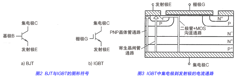
Obviously, these three paths can be regarded as parallel connection, as shown in FIG. 4A. After integration, the equivalent device circuit of IGBT is shown in Fig. 4B. Among them, the parasitic thyristor is composed of the parasitic NPN transistor in the MOS gate structure and the PNP transistor in the first channel. In practical application, to prevent the parasitic thyristor from thyristor effect causing device out of control and damage, that is, to suppress the role of NPN transistor, dotted line is used in the figure to indicate the unexpected NPN transistor. Regardless of the dotted line, IGBT can be regarded as a Darlington structure composed of n-channel MOSFET and PNP transistor, that is, the drain of MOSFET is connected with the base of PNP transistor.
Figure 4 IGBT equivalent circuit
At this point, we will compare the terminal naming in Figure 2 with the equivalent circuit in Figure 4, and we will find more interesting points in the naming of IGBT terminals. In the equivalent circuit, as the core of IGBT's main function, the equivalent transistor is PNP type. When the emitter of PNP transistor is connected to the outside of IGBT, it is called the collector of IGBT, and when the collector of PNP transistor is connected to the outside of IGBT, it is called the emitter of IGBT. According to the comparison of graphic symbols in Figure 2, this IGBT is equivalent to NPN Transistor (IGBT is designed to replace NPN Power Transistor), but In fact, the main equivalent transistor in IGBT is PNP type. The scientific and correct terminal naming of IGBT has puzzled many people.
Latest News
Contact Us
Email:info@dynpower.cn
Add:No. 77, Louyang Road, Suzhou Industrial Park
 qq
qq