knowledge
The basic working principle of junction field effect transis
The turn-on and turn off of Junction FET mainly depend on the control of conduction channel. Changing the bias voltage of the gate junction can change the expansion degree of the two space charge regions on both sides of the channel, thus changing the cross-section size of the channel, that is, changing the channel resistance, and the drain current will also change accordingly. The grid adopts voltage control, and the grid current can be very small to achieve the above changes. The extreme of these changes is that when the reverse bias voltage of the gate junction is large enough, the inner planes of the two space charge regions are joined together in the middle of the channel, which is conventionally referred to as the conductive channel is pinched off. At this time, there is no conductive channel between the source and the drain, and the operation of the junction field effect transistor is in the cut-off state, as shown in Figure 1.
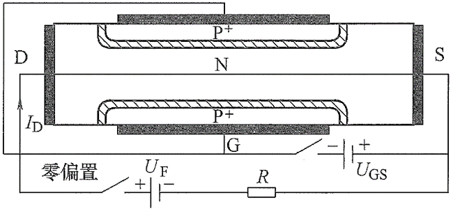
Figure 1 junction field effect transistor in off state
The turn-on of the junction field effect transistor can be simply regarded as the opposite of the cut-off state, that is, when the reverse bias of the gate junction is not large enough, zero bias or positive bias, a channel is generated in the space charge region of the gate junction to allow the current to pass through, the junction field effect transistor turns on. In fact, the conduction of junction field effect transistor is not so simple. With the increase of the flow current, it can be divided into four stages: linear, transition, saturation and breakdown, which are mainly affected by the voltage drop caused by the channel current.
In the practical application of junction field effect transistor, the reverse bias applied to the gate junction is relative to the source, that is, the common source connection method is adopted, and the control power supply and the common end of the main power supply are connected in the same source. Due to the high conductivity of heavily doped gate materials, the potential of each point in the region is basically the same, that is, the gate is regarded as an equipotential region. However, this is not the case in the channel. Because the channel material is light doped, its resistivity is high. When there is current flowing between the drain and the source, there must be a potential gradient, that is, voltage drop. At this time, the bias voltage on the gate junction is no longer evenly distributed, and the width of the gate junction space charge region is no longer equal from the drain to the source. Figure 2 shows the three stages.
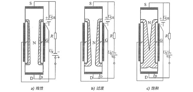
Fig. 2 conduction of Junction FET
1) Linear variation. When the current flowing through the junction field effect transistor is small, the potential gradient generated by the current in the channel is very small, which can be regarded as that the shape of the gate junction space charge region is affected very little, and the channel shape changes very little, as shown in Fig. 2A. In this case, it can be considered that the channel is a resistance region with fixed resistance value. The carrier drift motion in the channel satisfies Ohm's law, and the terminal voltage UDS changes linearly with the drain current ID.
2) Transition state. With the increase of drain current ID, the voltage drop in the channel increases, and the drain potential will be significantly higher than the source potential. Because the potential of the whole gate electrode is in reference to the source, the drain of the gate junction is in a reverse bias increasing state relative to the source. At this time, the space charge region of the gate junction gradually widens from the source to the drain, and the channel width correspondingly decreases, so the channel resistance increases, as shown in Fig. 2B. With the increase of UDS, this situation becomes more and more serious, and the deviation of ID from its linear value becomes larger and larger, which is called transitional state.
3) Saturation state. When the UDS voltage is higher than the transition region, the space charge regions on both sides of the channel will close from the drain end with the increase of UDS, and gradually advance the closing point to the source end slowly. The closure of the space charge region causes the conduction channel to be clamped off at the drain end. The essence of pinch off is that one end of the conductive channel becomes a space charge region where the carriers have been depleted, as shown in Fig. 2C. At this point, with the increase of UDS, Id no longer increases, which is called saturation state. It should be noted that there are essential differences between the higher UDS and the higher reverse bias UGS in the pinch off of conductive channels. The pinch off of higher reverse bias UGS is to make the whole conductive channel carrier exhausted, and the ID is zero; the pinch off of higher UDS only makes the drain end of the conductive channel partially depleted, and the electrons can still be swept through the space charge region and enter the drain by the strong electric field, so the ID is not zero, and the corresponding current is called saturation current.
4) Breakdown state. Once the drain end of the conductive channel becomes the space charge region, the rising of UDS will mainly fall in this high resistance region, where the electric field will become stronger and stronger, and the avalanche ionization effect of carrier multiplication in the space charge region will appear. As long as the UDS has a small increase, it will cause the sharp rise of ID, and eventually lead to device breakdown.
The output characteristics of the Junction FET and the relationship between UDS and ID under the action of UGS are shown in Figure 3. The segments corresponding to each state in the conduction are shown in the figure, which are linear region, transition region, saturation region and breakdown region respectively. In practical applications, Junction FET usually works in saturation region. The starting voltage (pinch off voltage) and ending voltage (avalanche breakdown voltage) of saturation region will decrease with the increase of the absolute value of gate voltage UGS. This is because the channel becomes thinner with the increase of gate voltage reverse bias, and the space charge region expands in the drain side.
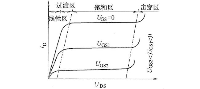
Figure 3 output characteristics of Junction FET
The n-channel junction field-effect transistor analyzed above is a depletion type field-effect device, which is called n-channel depletion type. In addition, there are three other types of junction field-effect transistors: p-channel depletion type, N-Channel Enhancement type and p-channel enhancement type. Their graphic symbols are shown in Figure 4.
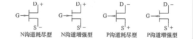
Figure 4 different types of symbols for junction field effect transistors
The depletion mode means that the device is normally on, and the enhancement mode means that the device is normally off. In contrast, the characteristics of each type of Junction FET are as follows:
1) N-channel depletion type. The conduction channel of n-channel depletion type is n-type, and the gate region is p + layer. When UGS = 0, there is a conductive channel and the channel resistance is small. Once a voltage is applied between the drain and the source, a large amount of current will flow through the channel. Only when the gate voltage is negative and high to a certain extent, the drain current ID will be cut off.
2) N-channel enhanced. The structure of n-channel enhanced mode is basically the same as that of n-channel depleted mode. However, when UGS = 0, the whole channel is occupied by gate junction space charge, the whole channel is clamped off, and the channel resistance is large. Therefore, even if a voltage is applied between the drain and the source, the channel current field is close to zero (that is, n-channel enhanced junction field effect transistor is a normally off device). Only when the positive gate voltage UGS is positively biased to a certain extent, the drain current ID begins to increase significantly.
3) P-channel depletion type. The p-channel depletion conduction channel is a p-type semiconductor, and the gate region is an N + layer. When UGS = 0, there is a conductive channel and the channel resistance is small. Once a voltage is applied between the drain and the source, a large channel current field will flow through the channel. Only when the gate voltage is positive and high to a certain extent, the drain current ID will be cut off.
4) P-channel enhanced. The structure of p-channel enhanced mode is basically the same as that of p-channel depleted mode. When UGS = 0, the whole channel is occupied by gate space charge, the whole channel is pinched off, and the channel resistance is large, so the channel current is close to zero. Only when the negative gate voltage is high to a certain extent, the drain current ID begins to increase significantly.
All of the above are long channel junction field effect transistors. The channel length of the long Channel Junction FET is much larger than the channel width, and the drain current is easily saturated due to the drain voltage clamping off the channel. The length and width of the channel can be compared, even smaller Junction FET belongs to short channel devices. For the application of power electronic converters, power field effect transistors are generally short channel devices.
Latest News
Contact Us
Email:info@dynpower.cn
Add:No. 77, Louyang Road, Suzhou Industrial Park
 qq
qq